Clash @LumiGuide
Reading time: 20 minutes
This blog article was written by Rowan Goemans.
LumiGuide is a company that specializes in bicycle and car detection systems. LumiGuide uses sensors to determine whether there are still free spots available for someone looking to park their bicycle or car. An important part of this system are the dynamic signs which keep everyone in the loop about where they can park their vehicle.

Figure 1: Sign part of the FRIS (Fiets-route-informatie-systeem) in Utrecht
Our first-generation signs boasted the integration of a Raspberry Pi coupled with a specialized daughterboard designed to control LED matrix panels. These LED matrix panels use a loosely defined protocol called HUB75. To drive these LED matrix panels well you need to be able to drive a 14-bit parallel interface racing at speeds of 25-30Mhz. The beloved Raspberry Pi struggled to deliver the required performance without significant compromises.
From Raspberry Pi to FPGA: LumiGuide’s Up-grade Journey
Having faced our challenges with the Raspberry Pi, we at LumiGuide were ready for an upgrade. Enter the FPGA (Field-Programmable Gate Array) for the second rendition of our Sign driver.
The DE0-Nano-SoC board caught our eye, and we paired it with a custom daughterboard. One of the defining features of this board is its integration of the Intel Cyclone V SoC FPGA. That means it has a hard ARM CPU capable of running Linux on it as well as an FPGA. The hard ARM CPU can communicate with the FPGA via built-in bridges. This made it possible to run a simple Python web server on the CPU which communicated with our own IP on the FPGA that handles driving the LED-matrices.
The first version was implemented in VHDL by LumiGuide’s then resident electronics engineer. In its nascent stage, it had a certain rustic charm – simple features, a modest refresh rate, and due to block RAM constraints, it could only power a handful of LED matrix panels concurrently. It’s essential to note these weren’t hardware limitations but more due to the initial design’s constraints.
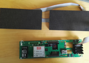
Figure 2: The DE0-Nano-SoC slotted inside the daughterboard
A few years after this I entered the picture at LumiGuide as a final project intern for my Embedded Software degree. By this time, our earlier electronics engineer, the VHDL expert, had embarked on a new journey elsewhere. The void left behind meant that LumiGuide was devoid of any hardware design expertise. This posed an operational challenge. An integral and yet unmaintainable component of our system was lying dormant, presenting not just a technical hiccup but a potential business risk.
So it was decided: my graduation project was to build the next version of the Sign driver.
Now, for some context: Haskell is LumiGuide’s go-to programming language. Given this foundation, our choice naturally fell on Clash as the underlying technology for the subsequent Sign driver. By leveraging Clash, we aimed not only to take back the reins of our sign driver but also to address the existing limitations and bugs.
I was about to enter a realm that was entirely alien to me. My knowledge base encompassed neither hardware design nor functional programming. Yet, this seemed like a really fun challenge where a lot could be learned. And oh boy did I learn a lot.
One of the best things about Clash is the extensive documentation available on Hackage. I cannot stress enough how invaluable that resource was while I was learning. Within my inaugural week, I managed to get the blinky example operational on the DE0-Nano-SoC. Yes, there were terms that went over my head initially (“PLL? Locked? What are those?”), but this was a perfect starting point for further iteration. Thanks to Clash’s lucid documentation and Haskell’s type safety, I could swiftly progress, piecing together knowledge on digital circuit design and functional programming.
My vision for the next generation Sign driver began to take shape. Instead of storing image in block RAM we would use the Hard Processor Systems(HPS) DDR3 SDRAM. Block RAM would only be used for ephemeral storage. At the same time control and status registers would go over the HPS2FPGA bridge. With this architecture in place, the limitation of the previous driver could be overcome.
Over the subsequent weeks, my primary focus was on bringing this new architec- ture to life. But, as with any endeavor, hurdles were bound to emerge. My main nemesis turned out to be Intel Quartus. Ensuring simultaneous access to the DDR3 SDRAM from both the FPGA and the HPS turned out to be not at all straightforward. Fortunately even with Intel Quartus doing it’s best to hinder my progress I had time to spare which allowed me to implement many of the wanted features that where previously impossible with the old Sign driver.
As this chapter of our journey came to a close, both LumiGuide and I reflected on our triumphs. This venture underscored the capabilities of Clash in the realm of hardware design. For someone who was treading this path for the first time Haskell’s static typing coupled with Clash’s exhaustive documentation proved to be a godsend. The ‘search by type’ feature offered by hoogle has saved me literal hours of manual lookups. My graduation project was a success and after I stayed with Lumi Guide as an employee.
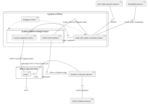
Figure 3: Architecture overview #1
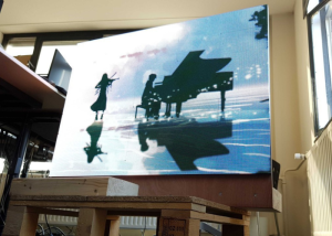
Figure 4: Demonstration of larger screens that the Sign driver could now support
New horizons
An exciting opportunity presented itself. LumiGuide clinched a pivotal contract to provide bicycle detection systems for ProRail in the Netherlands. For those unfamiliar with the Dutch landscape, ProRail is responsible for the rail infras-tructure in the Netherlands, which includes biycle parking amenities adjacent to train stations.
However, with great contracts come great responsibilities. The prospect of deploying hundreds, if not thousands, of signs over the ensuing years presented us with a challenge. Amplifying this challenge was a looming concern: the DE0-Nano-SoC board, the brains and heart of our sign driver, was being deprecated. With production ceasing, we had no choice but to go back to the drawing board.
During our exploration of alternatives, we found that China had its array of LED-matrix driver boards, some remarkably cost-efficient compared to our existing setup. These boards, dubbed “receiver cards,” were components of a complete proprietary system. This arrangement involved a “sender” card communicating with the aforementioned receiver cards via ethernet cables or sometimes fiber cables.
So we got to work to see whether we could use just these receiver cards with our own bitstreams as the core of our next-gen Signs.
It turns out that these receiver cards contain an 22K LUT Lattice ECP5 with dual gigabit Ethernet interface, some flash and SDRAM. The Lattice ECP5 is well-supported using open source Yosys and nextpnr. And since my previous stint showed me that I lost by far the most time with Intel Quartus, so the idea of trying a different flow with Yosys and nextpnr was refreshing.
Clash had been my trusty companion on previous ventures, so I was eager to harness its capabilities once more. A month of hacking resulted in a Proof-of-Concept, enabling us to display content on LED matrices via a rudimentary UART. Now it was time to go back to the drawing board on what requirements we had for this next-gen driver.
A crucial difference between the DE0-Nano-SoC and such a receiver card is that the DE0-Nano-SoC includes the ARM HPS. Which in our case ran Linux and exposed a simple Python based web API to upload content to. This is no go on the receiver card. They don’t contain a HPS. A soft core was too slow to handle the data rates involved for image streaming and processing. I opted for a design centered on a UDP-based request-response protocol. This could manage image data streaming into the FPGA, essentially standing in for the bridges we’d used with the DE0-Nano-SoC.
In contrast to the old implementation where the interfaces between components were all bespoke, here it was chosen to build most components on top of an AXI4-stream like protocol. This would allow greater flexibility and reusability of components and allow quicker circuit configuration. Below the new architecture.
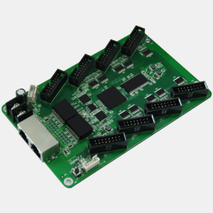
Figure 5: Colorlight receiver card
overview is given (excuse the abuse of UML state diagrams). The blue boxes are the components which process packets. The blue boxes between the Arbiter and Dispatcher are the endpoints which expose some interface we can talk to via UDP.
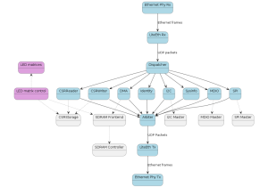
Figure 6: Architecture overview #2
With the desired architecture in place, it became clear we need two relatively complex components we did not have before. An SDRAM controller core and a Gigabit Ethernet core with UDP support. I delved into creating the SDRAM controller using Clash, a journey that I’ll detail further down the line. As for the Ethernet core, our research led us to liteeth. Which is part of the LiteX suite of cores which are completely open source and have extensive hardware compatibility. Like many other tools, liteeth was not without its gaps. While it provided a solid foundation, it lacked some crucial features that were indispensable for us. Together with enjoy-digital, the creator of LiteX, we worked to bring liteeth up to speed. Eager to bridge these gaps, we took the initiative to tailor the tool to our needs. We rolled up our sleeves and worked on most of the missing components. However, for a specialized requirement like initial DHCP support, we collaborated with enjoy-digital, leveraging their expertise to ensure seamless functionality.
The features that liteeth lacked and required our attention included:
- Core generator exposes Raw UDP interface. #1.
- DHCP support, #1, #2, #3.
- Dynamic link speed, #1.
- Gateway support, #1.
Herein lies the true strength of open source: it grants unparalleled flexibility. Unlike the rigid parameters of vendor IP, which often corner you into a “take it or leave it” situation, open-source platforms empower you with the choice and tools to customize to your own needs.
SDRAM controller
For the SDRAM controller we initially investigated whether litedram could suit our needs. Unfortunately litedram requires a softcore for initialization and does not support full-page burst, both features we wanted. Full-page burst allows a very simple and efficient way to burst a large amount of data into the SDRAM. Ideal for our use case where only large linear reads and writes are necessary.
While the idea of refining litedram, akin to our approach with liteeth, surfaced, we assessed the scope of the task. Realizing that an SDRAM controller is simpler and smaller in comparison to a full ethernet UDP stack, we saw an opportunity to craft our solution in Clash instead.
In Clash you can make circuits polymorphic over types. Since different SDRAM ICs have differing specifications in terms of timing we decided it would be a good fit to model the timings of SDRAMs on the type level and write the controller to be polymorphic in that specification. Below an example definition is given of a specific SDRAM IC. mkSDRAMModule does some magic so a lot of required constraints of the controller are proven in that function and then hidden in a GADT.
This term level value can then be used to instantiate a controller + crossbar for
that SDRAM IC adhering to all the timing parameters specified.
We are planning to eventually upstream this controller to Clash.Cores. But as of now there is still an unresolved clash compiler bug that needs to be addressed.
Once we had written the controller and validated the controller using unit tests we put it on the real hardware. It performed flawlessly in hardware at its very first trial. You might wonder why we choose to hide the tri-state nature of the SDRAM DQ lines. Different tools/FPGAs have different constraints for IO-registers and tri-state buffers. Keeping that separate from the controller allows users to handle that in the way required for their tooling.
Streams
Our choice to utilize an AXI4-lite like stream interface turned out to fit well. The core contract of this interface is the valid/ready handshake. The source (data transmitter) sends data + a valid signal, the sink(data receiver) asserts ready when it is able to receive data. Only when both valid and ready are asserted the handshake has occurred and the data has been transmitted.
The astute among you may know that QBayLogic is working on something exactly like this called clash-protocols. We chose to not use clash-protocols yet due to it not being released and generally missing documentation. So we wrote our own AXI lite stream types and utility functions. Once clash-protocols is released we plan to port our code over to it.
We modeled the content the stream source produces using a record + Maybe wrapper, hiding the valid bit. Let’s dive into the specifics of this record.
The most important operater being the |> operator, which allows one to connect components using this stream interface together.
Every packet is made of multiple StreamContent values and are delineated using the streamLast_ field. There is a distinction between metadata associated with a packet and the payload. The payload may change every single cycle. But the metadata is only allowed to change following the assertion of streamLast_.
For example, we are using UDP packets. Each UDP packet contains the following interesting information for us beside the payload of the packet:
- Source and Destination IP, 32-bit each.
- Source and Destination port, 16-bit each.
- Packet length, 16-bit.
Ofcourse these values do not change for a single packet so are a natural fit for storing in the metadata.
The rationale behind drawing a clear line between metadata and content is resource optimization. By storing and processing these parts of the stream separately, we can enhance the efficiency of buffering the stream using FIFOs.
A simplistic approach, where one lumps everything into a single FIFO, results in the instantiation of a wide FIFO, capable of accommodating payload, last, and metadata signals. However, this isn’t resource-efficient.
The proper solution is to use two separate FIFOs. The first FIFO stores the payload and the last signal, while the second focuses exclusively on metadata. With this bifurcation, the metadata FIFO can be considerably shallower than its payload counterpart, ensuring we avoid unnecessary waste of block RAM resources.
Coming together & Conclusion
In the dynamic world of technology, choosing the right technology for the job can become the blueprint for success. For us at LumiGuide Clash was this right technology. Giving us success in a field we were not experts in while also being a joy to use.
Following testing we rolled out the first bicycle parking detection system using these new Sign controllers in Naarden-Bussum.
Figure 7: Sign in Naarden-Bussum running a circuit developed in Clash
Looking ahead, the horizon is bright and promising. LumiGuide is gearing up to introduce hundreds of these state-of-the-art signs across the Netherlands. As travelers and locals alike witness these signs, it’s a silent testament to Clash’s instrumental role in bringing this vision to life.
Next time you spot one of these signs in the coming years, the chances are high you are looking at a piece of technology powered by Clash.
|
1 2 3 4 5 6 7 8 9 10 11 12 13 14 15 16 17 18 19 20 21 22 23 24 25 26 27 28 29 30 31 32 33 |
type SDRAMModuleDef dom spec = KnownDomain dom => 1 <= DomainPeriod dom => SDRAMMinPeriod dom spec <= DomainPeriod dom => DomainPeriod dom <= SDRAMMaxPeriod dom spec => KnownNat (DomainPeriod dom) => KnownNat (SDRAMDataWidth dom spec) => SDRAMModule dom spec -- | Specification for <https://www.esmt.com.tw/upload/pdf/ESMT/datasheets/M12L16161A(2R).pdf> type M12L16161A_5T rank = 'SDRAMSpec "M12L16161A-5T" ('ParamSDRAMDataWidth (rank * 16)) ('ParamSDRAMBanks 2) ('ParamSDRAMRows 2048) ('ParamSDRAMCols 256) ('ParamSDRAMtStartupDelay ('Picoseconds 200_000_000)) ('ParamSDRAMStartupRefreshes 2) ('ParamSDRAMtREFI ('Picoseconds 15_600_000)) ('ParamSDRAMtMRD ('Cycles 2)) ('ParamSDRAMtBDL ('Cycles 1)) ('ParamSDRAMtRP ('Picoseconds 15_000)) ('ParamSDRAMtRCD ('Picoseconds 15_000)) ('ParamSDRAMtWR ('Cycles 2)) ('ParamSDRAMtRFC ('Picoseconds 55_000)) ('ParamSDRAMCL 7000 ('Cycles 2) ('Cycles 3)) ('ParamSDRAMMinPeriod 5000) ('ParamSDRAMMaxPeriod 1000000) m12l16161a_5t :: forall rank dom . SDRAMModuleDef dom (M12L16161A_5T rank) m12l16161a_5t = mkSDRAMModule |
|
1 2 3 4 5 6 7 8 9 10 11 12 13 14 15 16 17 18 19 20 21 22 23 24 25 26 27 28 29 30 31 32 33 34 |
sDRAMFrontend :: forall (dom :: Domain) (spec :: SDRAMSpec) (ports :: Nat) . (KnownNat ports, 1 <= ports) => HasCallStack => KnownDomain dom => SDRAMModule dom spec -- ˆ The SDRAM module to instantiate the controller for -> Clock dom -- ˆ Clock input -> Signal dom (BitVector (SDRAMDataWidth dom spec)) -- ˆ The input DQ pins coming from the SDRAM IC. Must go through an IO -- register before being passed to this function. -> Signal dom (Vec ports (Maybe (BitVector (SDRAMDataWidth dom spec)))) -- ˆ Data supplied by user while writing -> Signal dom (Vec ports (Maybe (SDRAMRequest dom spec))) -- ˆ incoming requests. Requests are handled in a round-robin manner -- On a write request the first word to write must be supplied -> ( Signal dom (SDRAMCmd dom spec) , Signal dom (Maybe (BitVector (SDRAMDataWidth dom spec))) , Signal dom (Vec ports Bool) , Signal dom (Vec ports (Maybe (BitVector (SDRAMDataWidth dom spec)))) ) -- ˆ - The command output to the IC. Must be routed through IO registers. -- - Must be routed through a tri-state buffer + IO register. -- Applying `isJust` to this value results in the output enable of the tri-state -- buffer. -- - Ack of a write request. The user must start to stream data when ack -- is True. On the cycle following an ack they must provide the second -- word. On the next cycle the third word, etc. Until a full page has -- been written. -- - The data output of all ports, essentially the read request ack + data. -- It's guaranteed to transmit a full page consecutively. |
|
1 2 3 4 5 6 7 8 9 10 11 12 13 |
data StreamContent meta word = StreamContent { streamMeta_ :: meta , streamData_ :: word , streamLast_ :: Bool } deriving (Eq, Show, ShowX, Generic, NFDataX, BitPack) type StreamSource meta word = Maybe (StreamContent meta word) data StreamSink meta word = SinkNotReady | SinkReady deriving (Eq, Show, ShowX, Generic, NFDataX, BitPack) |
|
1 2 3 4 5 6 7 8 9 10 11 12 13 14 15 16 17 18 |
(|>) :: ( Signal domA (StreamSource metaA wordA) -> Signal domB (StreamSink metaB wordB) -> ( Signal domB (StreamSource metaB wordB) , Signal domA (StreamSink metaA wordA) ) ) -> ( Signal domB (StreamSource metaB wordB) -> Signal domC (StreamSink metaC wordC) -> ( Signal domC (StreamSource metaC wordC) , Signal domB (StreamSink metaB wordB) ) ) -> Signal domA (StreamSource metaA wordA) -> Signal domC (StreamSink metaC wordC) -> ( Signal domC (StreamSource metaC wordC) , Signal domA (StreamSink metaA wordA) ) |